")


Interline Transfer CCD sensor
A special advantage of this sensor type is the "electronic shutter" which makes it possible to create a great number of images per second and images with very short exposure times, as required for technical monitoring processes. For this purpose there is a further non-exposable pixel unit next to each light-active pixel which is capable of acting as a memory cell. The memory cell has a light-tight cover in order to make in insensitive to light.
After the exposure, the charges are shifted to the memory cells. From there the charge can be read out via the vertical and the single horizontal shift register(s), at the end of the chain it is amplified and converted into a voltage.
|
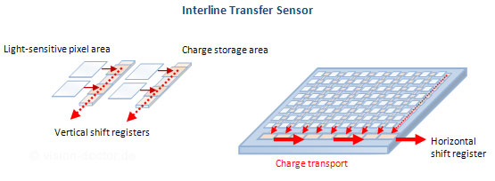
However, this functionality requires much space on the sensor which is not available for the actual image acquisition. The fill factor of the sensor is therefore only approximately 30 per cent. This main disadvantage of this construction variant could mostly be eliminated by using micro-lenses. For details see further down.
In case of this sensor, the image contents can be taken as a snapshot and buffered. While reading out, the next image can already be integrated. This behaviour of the sensor is ideal for short exposure times and the acquisition of continuous image sequences. The sensor can be operated at pixel clock frequencies of typically 20 to 60 MHz, with smaller pixels with fewer charge carriers (which have to be transported) allowing for a faster activation of the sensor. If the sensor is clocked too fast, the noise increases. This problem can be solved by reading out the sensor via two to four parallel readout channels (multi-tap camera).
Methods to increase the sensor sensitivity
The manufacturers of camera sensors always endeavour to increase the sensitivity, as this leads to an increase in image quality compared to competitors. This makes it possible to reduce sensor and pixel sizes and therefore increase the output of CCDs per wafer.
Micro-lenses
A method practised since the 1980s is the use of micro-lenses which are put onto each individual pixel structure on the semiconductor element. Especially interline transfer sensors require more space for not light-active structures on the surface of the CCD due to the horizontal and vertical shift registers for the transport of the sensor charges. By means of micro-lenses, a very high fill factor of 80 per cent and more can be achieved.
|
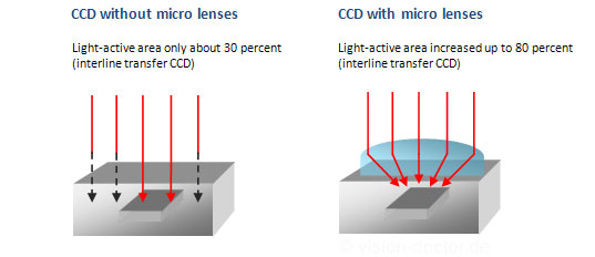
Micro-lenses to increase the sensitivity to light are used on almost all state-of-the-art IT-CCD sensors by Sony and Kodak/ TrueSense today.
Back-side illuminated sensors
A rather new technical design variant of CCD sensors of any type is the back-side illumination of the semiconductor, which are called BSI (back-side illuminated) sensors. The metallisation layers on the surface of the sensor to shift the charges towards the central A-D converter reduce the light-sensitive surface. For this purpose, the sensor must only be put upside down onto a support material and be exposed. In order to bring this effect about, the silicon layer of the sensor must whetted extremely thin, which results in higher production costs, a greater number of defective goods and higher sensor prices. The sensitivity of such a sensor is in some cases twice as high as that of a front-side illuminated CCD.
Modern representatives with high sensitivity and good image quality are, for example, the 1.4 megapixel sensor Sony CCD ICX285, Sony ICX625 (5 MPix), Sony ICX694 (6 MPix), TrueSense (Kodak) KAI-08050 (8 MPix) oder KAI-29050 with 29 megapixels.