CCD sensors
The term "CCD" means "charge-couple device" and is an electronic module which is capable to transport electronic charges.
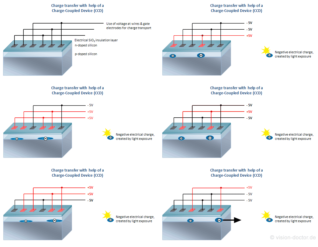
This technology was invented in 1969 in the Bell Laboratories by Willard Boyle and George E. Smith as pure data storage possibility, for storage purposes, however, it never gained technical acceptance. Yet this principle has still successfully been used until today in order to transport charges generated by exposing a semiconductor due to the "inner photon effect" by means of a great number of small steps (vertical and horizontal shift registers) to a central A/D converter, i.e. using a sort of "bucket chain principle". The charge shifting by means of electrodes is forced from the outside by applying electric potentials:
|
(Willard Boyle and George E. Smith received the Nobel Prize in Physics in 2009 for this fundamentally important invention 40 years after the discovery of this effect.)
An image sensor which makes use of this principle to shift and read out the charges of the light-active pixels is called "CCD sensor".
The frequency, i.e. how often per second the sensor is capable to transport the charge by one pixel, is called "pixel clock". The frequencies at which CCDs are operated today are approximately 25 to 50 MHz.
Simplified functional principle of the sensitivity to light
The inner photoelectric effect is fundamental for the functioning of the sensor.
The atoms of the silicon crystal are located on discrete energy bands, the energetically lower is called valence band, the energetically higher is called conduction band. In the basic state, most of the electrons are on the valence band, however they can be transported to the conduction band by means of excitation from the outside.
The energy required for this is 1.26 eV or more. In case of the CCD sensor, this transport can be induced by light, but also by higher heat supply (dark noise of the sensor). (Note: 1.26 eV approximately correspond to the energy of infrared radiation with a wavelength of 1 µm. Light with longer waves can pass through the silicon without absorption, it is virtually translucent from these wavelengths on and insensitive.)
Due to the excitation, free (negative) electrons and positively charged "holes" in the valence band are created at the same time which separate from each other because of the applied voltage. These charges, however, do not immediately flow off to the outside (like in the case of a photo diode in the CMOS sensor), but are stored in the memory cell itself.
By means of the charge shifting described above, the charge is transported through the entire sensor in many small steps towards a central amplifier / A-D converter.
Typical layout of CCD sensors
In general we differentiate several typical CCD sensor layouts which are described subsequently:
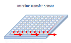
of which mainly the so-called "interline transfer sensor" has gained acceptance in machine vision.
|
Only this one can capture very fast frame rates by means of an "electronic shutter function" and is therefore used in 90 per cent of the industrial CCD cameras for machine vision.
Frame transfer CCDs and full frame transfer CCDs are mainly used in scientific applications with low image refresh rates today, where extremely high sensitivity to light is the main criterion.
Advantages and disadvantages of the CCD sensor technology
As the conversion of the charge in voltage is done by one central amplifier / A-D converter for all pixels, there are many advantages and disadvantages compared to CMOS sensors:
Advantages
- Higher sensitivity and lower noise due to enhanced surface use (higher fill factor)
- Fewer defective pixels due to the simpler structure
- Better image homogeneity thanks to the central A/D converter
Disadvantages
- Slower readout, as only one central A/D converter digitalises
- No direct pixel access, like in case of the CMOS sensor, as the CCD sensor must be read out serially
- More complex camera layout due to required additional electronics leads to larger and more expensive cameras
- Higher energy consumption of the entire camera
- More smearing and blooming effects when overexposing compared to a CMOS sensor
Important for machine vision
- In the majority of industrial applications, cameras with CCD sensors are used. They are low in noise, sensitive to light, have a high uniformity and, due to their linear characteristic, suitable for precise measuring applications.
- An overwhelming majority of manufacturers of industrial cameras use CCD sensors in their standard products, which are made by Sony in 90% of the cases. New and advanced sensors have been brought to market again and again over the years. If you have particularly high sensor requirements, check whether a newer or older sensor variant is used.
- Due to enhanced production technologies, higher sensitivities of the pixels are achieved which in turn allow for smaller and smaller pixel sizes (maintaining the same quality). The quality requirements for the optics have therefore risen extremely.
- CCD sensors with particularly fast frame rates or a particularly high resolution are developed by Kodak (since 2011: TrueSense). Here a look at the data sheet is worthwhile, too, to see which type (new / old variant) is used.
- Almost every sensor has a certain number of defective pixels which are hardly apparent most of the time and can sometimes be eliminated by the camera firmware by means of pixel error correction. CCD manufacturers typically differentiate their sensors in the quality grades "B", "A" and "zero" in order to describe the number of defective pixels. They vary in price. In case of extremely critical applications, you can buy cameras of grade "zero" with zero defective pixels from certain camera manufacturers at a surcharge.
- Approximately with every 6 degrees of temperature rise, the thermal noise of the pixels doubles. Good cameras should not become particularly warm during operation. Besides, avoid mounting the camera in a heat accumulation zone.


